Chapter 11 Serial Interface 0, 1
XI - 16
Control Registers
Serial Interface 1 Mode Register 1 (SC1MD1)
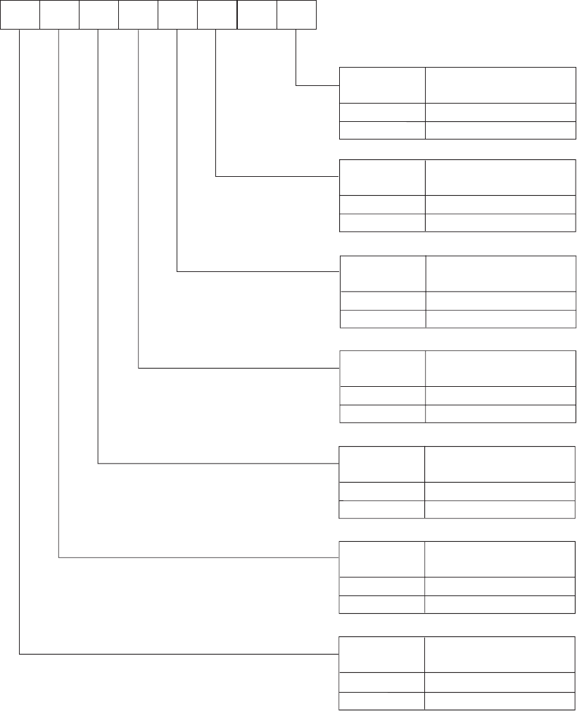
Figure 11-2-12 Serial Interface 1 Mode Register 1 (SC1MD1 : x'03F9B', R/W)
0124
567
3
(At reset : 0 0 0 0 0 0 - 0 )
SC1MD1
SC1CMDSC1MSTSC1CKMSC1SBOS
SC1SBISSC1SBTSSC1IOM
0
1
Synchronous serial
Synchronous serial /
Duplex UART selection
Duplex UART
SC1CMD
0
1
Clock slave
Clock master /
slave selection
Clock master
SC1MST
0
1
Data input from SBI1(RXD1)
Serial data I/O selection
Data input from SBO1(TXD1)
SC1IOM
-
0
1
Port
SBT0 pin function selection
Transfer clock I/O
SC1SBTS
0
1
"1" input
Serial input control
Serial input
SC1SBIS
0
1
Port
SBO0(TXD0) pin function
selection
Serial data output
SC1SBOS
0
1
Do not divide by 8
1/8 dividing of transfer clock
selection
Divide by 8
SC1CKM


