


Chapter 12 Serial Interface 3
Operation
XII - 30
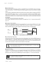
Clock Setup
The transfer clock of IIC communication is the one that the clock source is divided by 3 inside of this
serial. The clock source is selected from the dedicated prescaler and timer 5 output by the SC3CKS
register. But clock source should be set so that the transfer rate is not over 400 kHz. The dedicated
prescaler starts as the PSCMD (x'03F6F') register selects "prescaler operation". Set the SC3MST flag of
the SC3MD1 register to "1" to select the internal clock (clock master), always. This IIC interface can not be
used as the external clock (clock slave).
Transfer Format
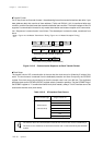
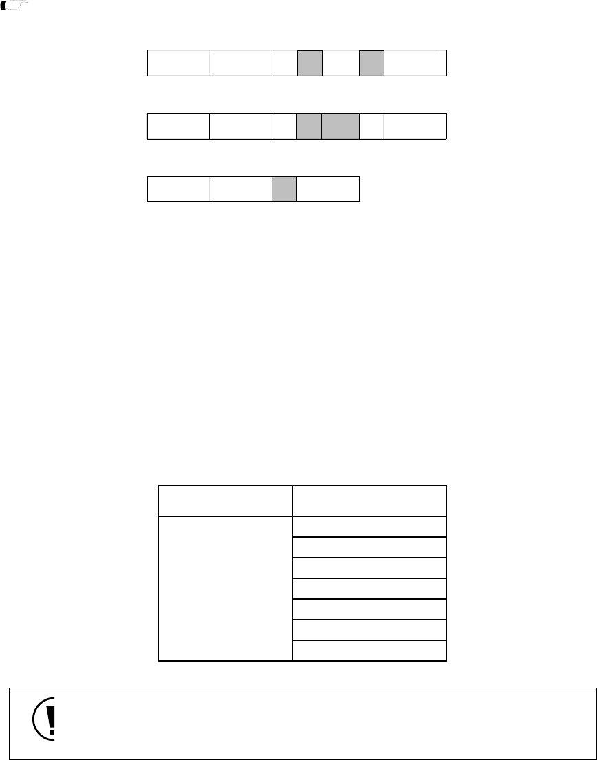
On IIC bus, there are 2 transfer formats : the addressing format that transmits/receives data after 1 byte
data (address data) that consists of slave address (7 bits) and R/W bit (1 bit) is transferred after start
condition, and the free data format that transmits data after start condition. The serial interface of this LSI
supports 2 communication formats for only master transmission and master reception at IIC communica-
tion. Sequence of communication is as follows. The shaded part is shown the data, transferred from
slave.
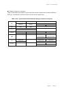
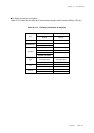
Figure 12-3-15 Communication Sequence on Each Transfer Format
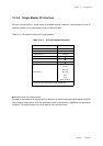
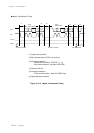
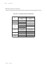
Table 12-3-12 IIC Interface Clock Source
The transfer rate at IIC communication should be the one that clock source is divided by 3.
The clock source should be set so that the transfer rate is under 400 kHz by the SC3CKS
register.
[ Figure 12-3-16 Master Transmission Timing, Figure 12-3-17 Master Reception Timing ]
Start
condition
data
Stop
condition
ACK
Start
condition
Slave
address
R/W
no
ACK
Stop
condition
ACK
data
Start
condition
Slave
address
R/W
data
Stop
condition
ACK
ACK
Free data format (master transmission)
Addressing format (master transmission)
Addressing format (master reception)
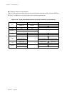
Communication type Single master IIC
fosc/2
fosc/4
Clcok source fosc/16
(internal clock) fosc/32
fs/2
fs/4
timer 5 output