


Chapter 12 Serial Interface 3
Operation
XII - 29
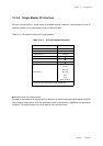
SDA
SCL
12
. .
8
ACK bit reception clock
(generated by switching
the pin of software)
ACK/
NACK
Data transmission period
(Hardware processing period)
Interrupt
ACK bit reception period
(Software processing period)
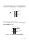
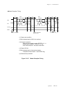
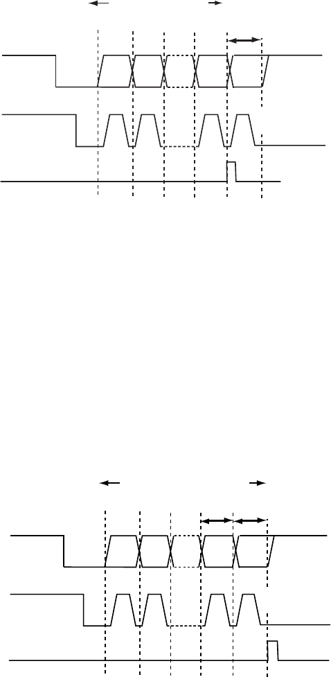
Figure 12-3-13 ACK Bit Reception Timing after Transmission of 8-Bit Data
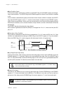
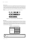
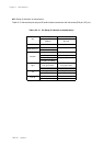
Figure 12-3-14 ACK Bit Transmission Timing after Reception of 8-Bit Data
SDA
SCL
12
. .
8
ACK bit transmission clock
T
Tmax=1.2 T
ACK/
NACK
Data reception period
(Bus release period)
Interrupt
Reception of Acknowledgement (ACK) Bit after Data Transmission
This LSI does not contain the function of receiving the acknowledgement (ACK) bit after data transmission.
To receive ACK bit after transmitting data, select sc3acks= "0" (No ACK bit) before data transmisison. By
transmitting the 8-bit data, an interrupt generates. Then switch the SBT pin function to "port" in the interrupt
routine. With the port function, program a clock for ACK reception and read the ACK data.
Transmission of Acknowledgement (ACK) bit after Data Reception
The way of the selection if ACK bit is enabled or not is the same to the way at the transmission. When
ACK bit is enabled, ACK bit and clock are output after data (1 to 8 bits) is received. If the reception is to
continue, ACK bit outputs "L". And if the reception is to finish, it outputs "H". The SC3ACK0 of the
SC3CTR register sets the output ACK bit level.