


II - 25
Chapter 2 CPU Basics
Clock Switching
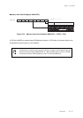
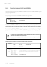
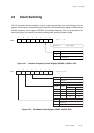
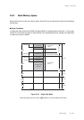
Figure 2-5-2 CPU Mode Control Register (CPUM : x'03F00', R/W)
2-5 Clock Switching
This LSI can select the best operation clock for system by switching clock cycle division factor by
program. Division factor is determined by both flags of the CPU mode control register (CPUM) and the
Oscillator frequency control register (OSCMD). At the highest-frequency, CPU can be operated in the
same clock cycle to the external clock hence providing wider operating frequency range.
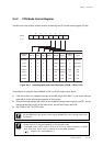
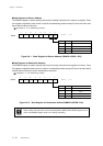
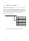
Figure 2-5-1 Oscillator Frequency Control Register (OSCMD : x'03F2D', R/W)
SOSC2DS
0
7654321
0
( At reset : - - - - - - 0 0 )
SOSC2DS
------
Reserved
Low-frequency Clock
Standard (Input the oscillation clock cycle)
Divided (Input the oscillation clock cycle
divided by 2)
Reserved
Set "0", always.
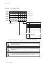
OSCMD
1
OSCDBL
0
7654321
0
CPUM
( At reset : 0 0 0 0 0 0 0 0 )
OSC1OSCSEL1 OSCSEL0 OSCDBL STOP
HALT
OSC0
Internal System Clock
Standard (Input the oscillation clock cycle
divided by 2)
2x-speed (Input the oscillation clock cycle)
0
0
1
1
0
1
0
1
1
4
16
64
1
4
16
16
Division factor
NORMAL mode SLOW mode
OSCSEL1 OSCSEL0
SOSCDBL
1
SOSCDBL
Low Speed Oscillation Clock
Standard (Input the oscillation clock cycle
divided by 2)
2x-speed (Input the oscillation clock cycle)
1
0