


Chapter 1 Overview
I - 18
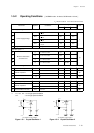
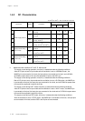
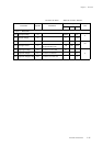
Electrical Characteristics
1-5 Electrical Characteristics
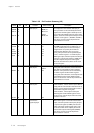
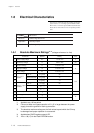
*1 Applied to any 100 ms period.
*2 Connect at least one bypass capacitor of 0.1 µF or larger between the power
supply pin and the ground for latch-up prevention.
*3 The absolute maximum ratings are the limit values beyond which the LSI may
be damaged and proper operation is not assured.
*4 Applied when P8LED register outputs LED.
*5 -40 to + 98 (°C) for the Flash EEPROM version.
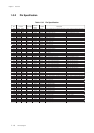
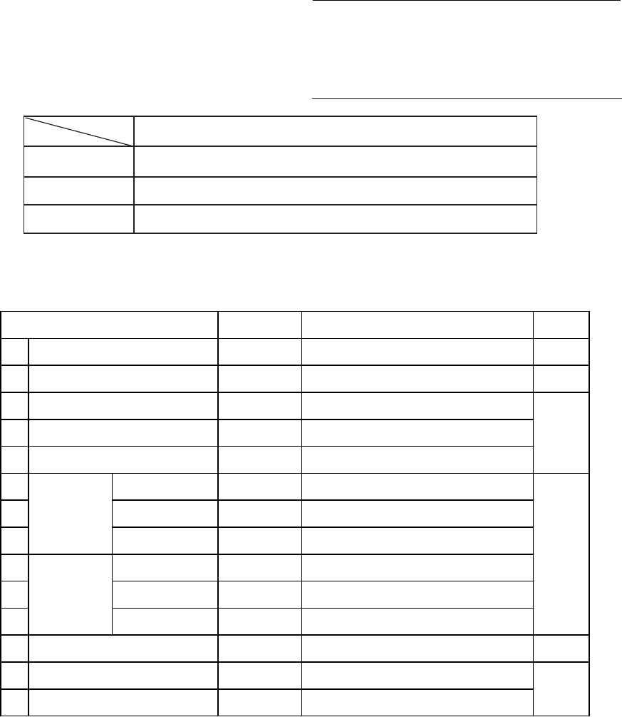
1-5-1 Absolute Maximum Ratings
*2,*3
(voltages referenced to Vss)
This LSI user's manual describes the standard specification.
System clock ( fs ) is 1/2 of high speed oscillation at NOR-
MAL mode, or 1/4 of low speed oscillation at SLOW mode.
Please ask our sales offices for its own product specifica-
tions.
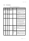
Contents
Structure
Application
Function
Model
MN101C77
CMOS integrated circuit
8-Bit single-chip microcontroller
General purpose
1
2 Input clamp voltage
3
4
5
6
7
8
9
10
11
12
13
14
V
µ
A
- 0.3 to +4.6
V
I
-0.3 to V
DD
+0.3
-0.3 to V
DD
+0.3
UnitRating
Ic -500 to +500
VPower supply voltage
Symbol
V
DD
Parameter
20
Input pin voltage
Output pin voltage
I/O pin voltage
Peak output
current
Port 8 *4
Other than Port 8
-40 to +85
V
O
V
IO
I
OL2
(avg)
I
OL1
(peak)
I
OL2
(peak)
I
OH
(peak)
I
OL1
(avg)
-0.3 to V
DD
+0.3
30
mW
Operating ambient temperature
Storage temperature
P
D
Power dissipation 300
T
opr
T
stg
-40 to +125 *5
o
C
mA
Average output
current *1
Port 8 *4
Other than Port 8
I
OH
(avg) -5
5
10
-10