


Operation
Chapter 15 A/D Converter
XV - 13
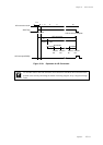
Setup Procedure Description
(7) Set the ANLADE flag of the A/D converter
control register 0 (ANCTR0) to "1" to send a
current to the ladder resistance for the A/D
conversion.
(8) Set the ANSTSEL flag of the A/D converter
control register 2 (ANCTR2) to "0", and select
"writing to the ANST flag of the A/D converter
control register 2 (ANCTR2)"as the A/D
converter activation factor.
(9) Set the ANST flag of the A/D converter control
register 2 (ANCTR2) to "1" to start the A/D
conversion.
(10) When the A/D conversion is finished, the A/D
conversion complete interrupt is generated
and the ANST flag of the A/D converter control
register 2 (ANCTR2) is cleared to "0". The
result of the conversion is stored to the A/D
converter buffer (ANBUF0, 1).
Note : The above (3) to (4) can be set at once.
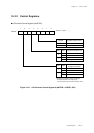
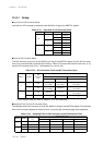
(7) Set the A/D ladder resistance.
ANCTR0 (x'3FB0')
bp3 : ANLADE = 1
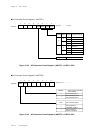
(8) Start the A/D conversion.
ANCTR2 (x'3FB2')
bp6 : ANSTSEL = 0
(9) Start the A/D conversion operation.
ANCTR2 (x'3FB2')
bp7 : ANST = 1
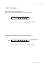
(10) Complete the A/D conversion.
ANBUF0 (x'3FB3')
ANBUF1 (x'3FB4')
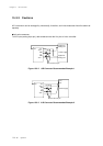
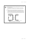
Start the A/D conversion after the current flowing through the ladder resistors stabilizes. The
wait time should be decided by the caluculated times from the ladder resistance (max. 80
kΩ), and the external bypass capacitor connected between VREF+ and VREF-.