


XI - 25
Chapter 11 Serial Interface 0, 1
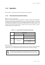
Operation
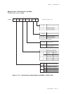
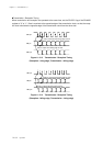
Data Input Pin Setup
3 channels type (clock pin (SBT pin), data output pin (SBO pin), data input pin (SBI pin)) or 2 channels
type (clock pin (SBT pin), data I/O pin (SBO pin)) can be selected as the communication. SBI pin can be
used for only serial data input. SBO pin can be used for serial data input or output. The SCnIOM flag of
the SCnMD1 register can select if the serial data is input from SBI pin or SBO pin. When "data input from
SBO pin" is selected to set the 2 channels type, the PnDIR0 flag of the PnDIR register controls direction
of SBO pin to switch transmission / reception. At that time, SBI pin is free to be used as a general port.
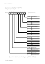
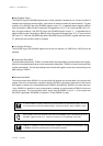
Clock Setup
The SCnCKS register selects a clock source from the special prescaler and timer 4 output. The special
prescaler starts its operation after the PSCMD (x'03F6F') register selects "prescaler operation". The
SCnMST flag of the SCnMD1 register can select the internal clock (clock master), or the external clock
(clock slave). Even if the external clock is selected, set the internal clock that has the same clock cycle
or below to the external clock, by the SCnCKS register. That is happened, because the interrupt flag
SCnTIRQ is generated by the internal clock. Here is the internal clock source that can be set by the
SCnCKS register. Also, the SCnCKM flag of the SCnMD1 register can divide the internal clock by 8.
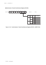
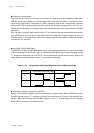
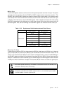
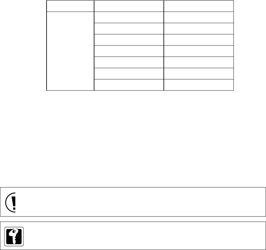
Table 11-3-3 Synchronous Serial Interface Internal Clock Source
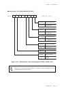
The transfer speed should be up to 2.5 MHz. If the transfer clock is over 2.5 MHz, the
transmission data may not be sent correctly.
At reception, if SCnIOM of the SC0MD1 register is set to "1" and "serial data input from SBO"
is selected, SBI pin is used as a general port.
Serial interface 0 Serial interface 1
fosc/2 fosc/2
fosc/4 fosc/4
fosc/16 fosc/16
fosc/64 fosc/64
fs/2 fs/2
fs/4 fs/4
Timer 5 output Timer 4 output
Internal clock