


XI - 21
Chapter 11 Serial Interface 0, 1
Operation
11-3 Operation
Serial Interface 0, 1 can be used for both clock synchronous and duplex UART.
11-3-1 Clock Synchronous Serial Interface
Activation Factor for Communication
Table 11-3-1 shows activation factors for communication. At master, the transfer clock is generated by
setting data to the transmission data buffer TXBUFn, or by receiving a start condition. Except during
communication, the input signal from SBT0 pin is masked to prevent errors by noise or so. This mask
can be released automatically by setting a data to TXBUFn(access to the TXBUFn register), or by
inputting a start condition to the data input pin. Therefore, at slave, set data to TXBUFn, or input an
external clock after a start condition is input.
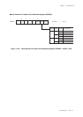
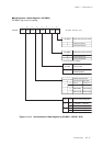
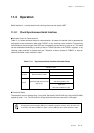
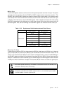
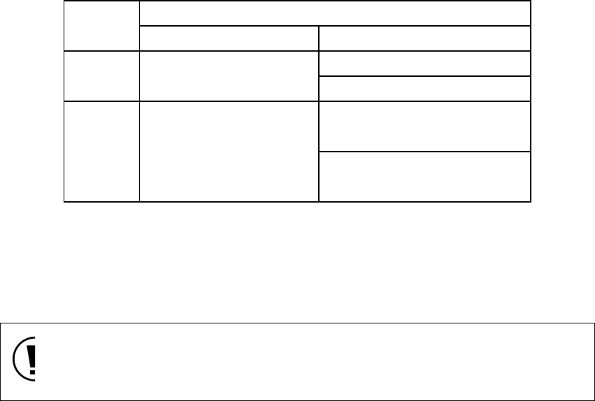
Table 11-3-1 Synchronous Serial Interface Activation Factor
Transfer Bit Setup
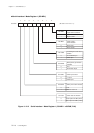
The transfer bit count is selected from 1 bit to 8 bits. Set them by the SCnLNG 2 to 0 flag of the SCnMD0
register (at reset : 111). The SCnLNG 2 to 0 flag holds the former set value until it is set again.
Except during communication, SBT pin is masked to prevent errors by noise. At slave com-
munication, set data to TXBUFn or input a clock to SBT pin after a start condition is input.
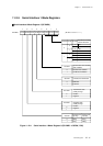
Transmission Reception
Set dummy data
Input start condition
Input clock
after dummy data is set
Input clock
after start condition is input
Activation factor
at master Set transmission data
Input clock after transmission
data is set
at slave